Graphene FET chip
S10
Manufacturer: Sigma Aldrich
Synonym(S): Graphene FET, Graphene FET sensor, Graphene FET with 30 Hall-bar devices and 6 2-probe configurations with varied channel geometry
Select a Size
| Pack Size | SKU | Availability | Price |
|---|---|---|---|
| 1 EA | GRFETS10-1-EA | In Stock | ₹ 49,510.00 |
GRFETS10 - 1 EA
In Stock
Quantity
1
Base Price: ₹ 49,510.00
GST (18%): ₹ 8,911.80
Total Price: ₹ 58,421.80
description
Dirac point:< 50 V Gate Oxide material: SiO2Gate Oxide thickness: 90 nmGraphene field-effect mobility: >1000 cm2/V·sMaximum gate-source voltage: ± 50 VMaximum temperature rating: 150 °CMaximum drain-source current density: 107 A/cm2Metallization: Chromium 2 nm/Gold 50 nmMonolayer CVD grown Graphene based field effect transistors (FET) S10Residual charge carrier density: <2 x 1012 cm-2Resistivity of substrate: 1-10 Ω·cmYield >75%
Related Products


Description
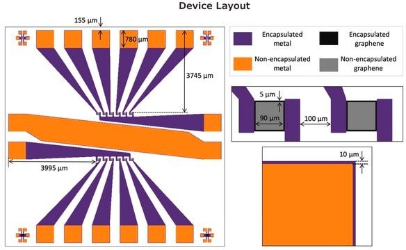
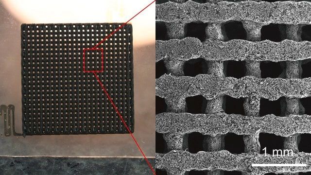
- General description: Device configuration:This Graphene FET chip provides 36 graphene devices distributed in a grid pattern on the chip. 30 devices have Hall-bar geometry and 6 have 2-probe geometry. The Hall-bar devices can be used for Hall measurements as well as 4-probe and 2-probe measurements. There are graphene channels with varied dimensions to allow systematic investigation of device properties.
- Application: Graphene device research[4]FET based sensor research for active materials deposited on graphene[5]Chemical sensors[5]Biosensors[6]Bioelectronics[6]Magnetic sensorsPhotodetectors
- Features and Benefits: Device Features:State-of-art graphene FETs utilizing consistent high-quality CVD grown monolayer grapheneDevices are not encapsulated and can be functionalized by additivesPerfect platform for sensor research and development36 individual graphene FETs per chipMobilities typically > 1000 cm2/V·s
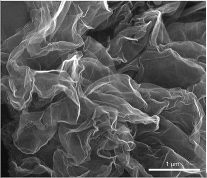
- Caution: Basic handling instructions:The monolayer CVD graphene used in this FET device is highly prone to damage by external factors.To maintain the quality of the devices, we recommend taking the following precautions:Be careful when handling the graphene FET chip.Tweezers should not contact the device area directly.
SAFETY INFORMATION
WGK
nwg
Flash Point(F)
Not applicable
Flash Point(C)
Not applicable