Graphene FET chip
S20
Manufacturer: Sigma Aldrich
Synonym(S): 2-probe FET device, 2-probe Graphene FET sensor, Chemical gated Graphene FET, GFET S20, Graphene field effect transistor chip S20
Select a Size
| Pack Size | SKU | Availability | Price |
|---|---|---|---|
| 1 EA | GRFETS20-1-EA | In Stock | ₹ 48,470.00 |
GRFETS20 - 1 EA
In Stock
Quantity
1
Base Price: ₹ 48,470.00
GST (18%): ₹ 8,724.60
Total Price: ₹ 57,194.60
description
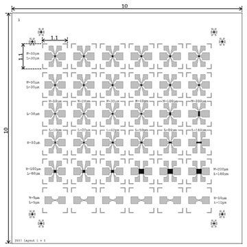
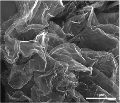
Absolute Maximum RatingsMaximum gate-source voltage: ± 50 VMaximum temperature rating: 150 °CMaximum drain-source current density: 107 A/cm2Chip dimensions: 10 mm x 10 mmChip thickness: 675 μmDirac point: < 50 VYield >75%Encapsulation: 50 nm Al2O3 + 100 nm Si3N4Gate oxide materials: 90 nm SiO2Graphene field-effect mobility: >1000 cm2/V·sMonolayer CVD grown Graphene based 2-probe field effect transistors (FET).Number of devices per chip: 12Resistivity of substrate: 1-10 Ω·cmMetallization: Chromium/Gold-Palladium 2/50 nm
Related Products


Description
- General description: Device configuration:The graphene FET-S20 chip is designed for measurements in liquid medium. This chip provides 12 graphene devices, with encapsulation on the metal pads to avoid degradation and reduce leakage currents, and the probe pads located near the periphery of the chip. It also includes a non-encapsulated electrode at the center of the chip, which allows liquid gating without the need of an external gate electrode.
- Application: Bioelectronics[3]FET based sensor research for active materials deposited on graphene[4]Clinical applications[5]Biosensors[6][7]
- Features and Benefits: Device Features:State-of-the-art GFETs utilizing consistently high-quality CVD monolayer grapheneMetallic contacts and metal/graphene interface are encapsulated to avoid degradation and reduce leakage current in liquid environmentPerfect platform device for new sensor research and development12 individual GFETs per chipA central gate electrode
SAFETY INFORMATION
WGK
nwg
Flash Point(F)
Not applicable
Flash Point(C)
Not applicable